The solar energy direct conversion into electrical energy uses the physical phenomenon called photovoltaic effect of light radiation with valence electrons interaction in semiconductor media.
In conventional crystalline silicon cell case, 4 of the normally silicon atom 14 electrons are valence atoms and therefore can participate in interactions with other atoms (both silicon and other elements).
Two adjacent pure silicon atoms have a pair of electrons in common.
There is a strong electrostatic bond between an electron and the two atoms it helps together hold.
That link can be separated by a certain energy amount.
If the supplied energy is sufficient, the electron is brought to a higher energy level (conduction band), where it is free to move.
When it passes to the conduction band, the electron leaves a “hollow” behind, that is to say a vacuum where an electron is missing. A nearby electron can easily fill the gap, thus exchanging space with it.
To take advantage of electricity it is necessary to create a coherent electrons movement (and voids) by an electric field inside the cell.
The field is formed with physical and chemical treatments that create an excess of positively charged atoms in one part of the semiconductor and an excess of negatively charged atoms in the other.
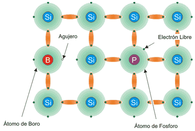
This is obtained by introducing small amounts of boron (positively charged) and phosphorus (negatively charged) atoms into the silicon crystalline structure, ie doping the semiconductor.
The electrostatic attraction between the two atomic species creates a fixed electric field that gives the cell the so-called diode structure, in which the current passage is obstructed in one direction and facilitated in the opposite one.
In phosphor doped layer, which has 5 outer electrons against the 4 silicon, a negative charge formed by a valence electron is present for each phosphorus atom.
In doped layer with boron, which has 3 outer electrons, a positive charge formed by the voids present in boron atoms when combined with silicon is created.

The first layer, negative charge, is denoted by N; the other, positively charged, with P; the separation zone is called P-N junction.
When the two layers are approached, an electronic flow is activated from the N zone to the P zone, which, when the electrostatic equilibrium is reached, determines a positive excess of charge in the N zone and an excess of negative charge in zone P.
The result is a device internal electric field that separates the excess electrons generated by the absorption of the light in the corresponding holes, pushing them in opposite directions (the electrons towards the zone N and the holes towards the zone P) so that a circuit can collect the current generated.
Therefore, when light hits the photovoltaic cell, positive charges are pushed in increasing numbers towards cell top and negative charges towards the bottom, or vice versa, depending on cell type.

If lower and upper part are connected by a conductor, the free loads pass through it and an electric current is obtained.
While the cell remains light exposed, electricity flows regularly as direct current.
Conversion efficiency in commercial silicon cells normally ranges from 13% to 20%.
Typical photovoltaic cell has a total thickness of between 0.25 and 0.35 mm.
It is generally square in shape, has a surface area between 100 and 225 mm² and produces (with a radiation of 1 kW / m² at a temperature of 25 ° C) a current between 3 and 4 A, a voltage of approximately 0.5 V and a corresponding power of 1.5-2 Wp.
This is an extract of contents included in Technical-Commercial Photovoltaic Solar Energy Manual and e-learning training of Sopelia.
Solar energy wherever you are with Sopelia.
